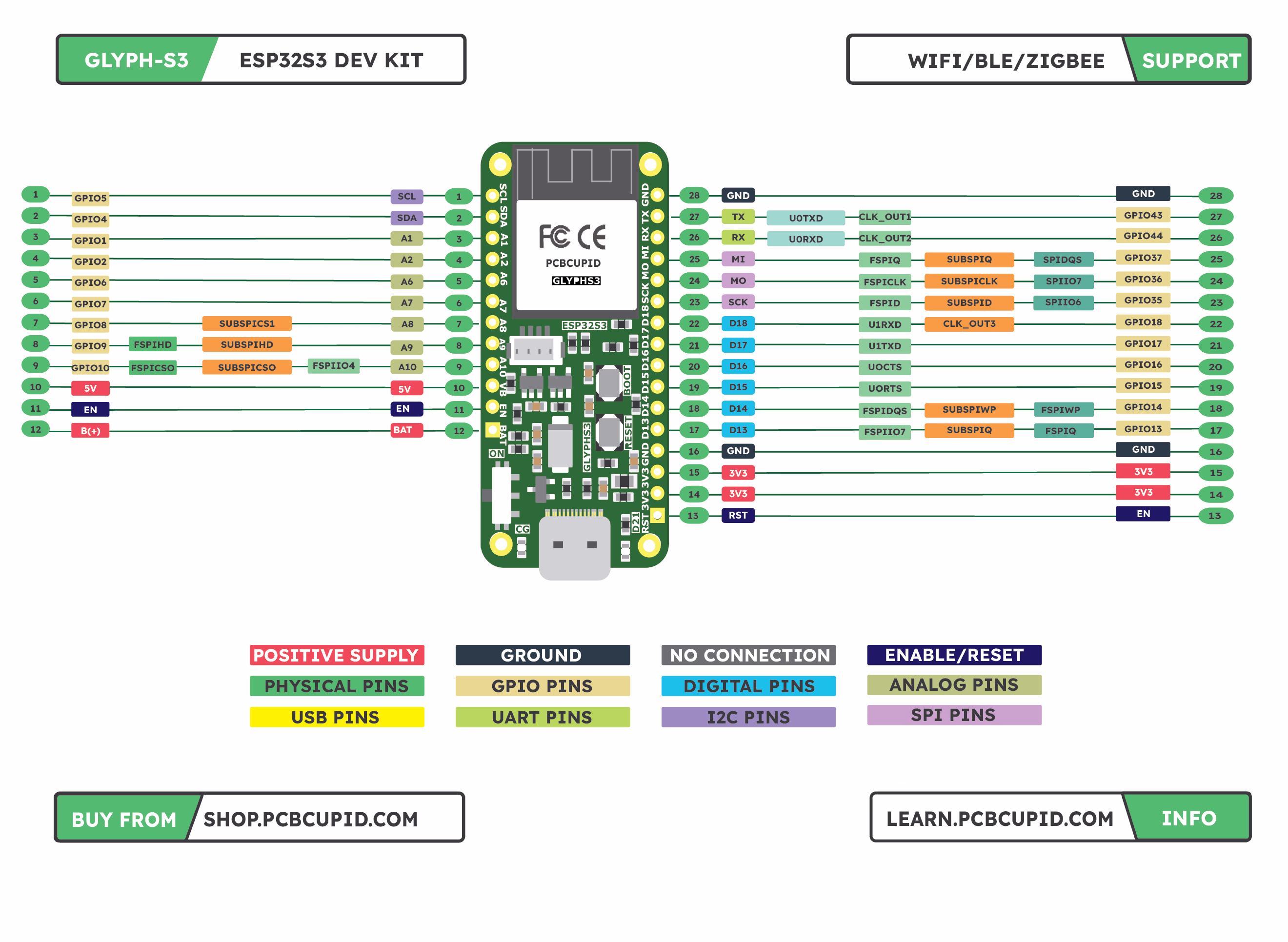
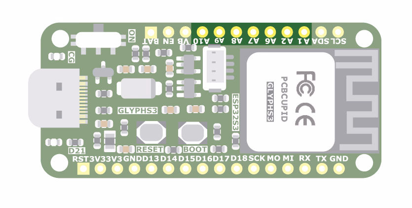
CLICK HERE TO DOWNLOAD HD CLICK HERE TO DOWNLOAD PDF The Glyph S3 has many pins, ports, and features. This page takes you on a tour on each of the pin on the board!
Power Pins and Connections
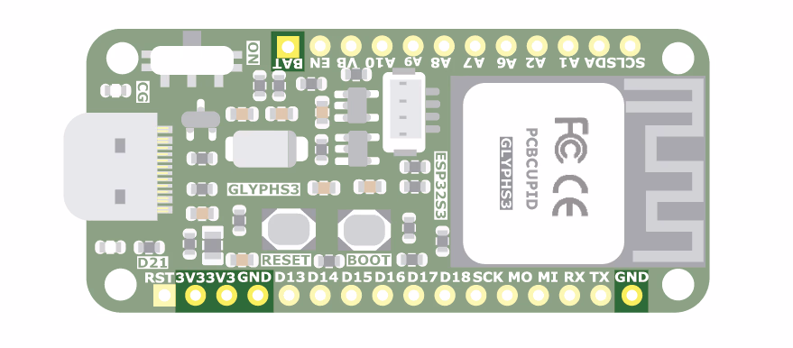
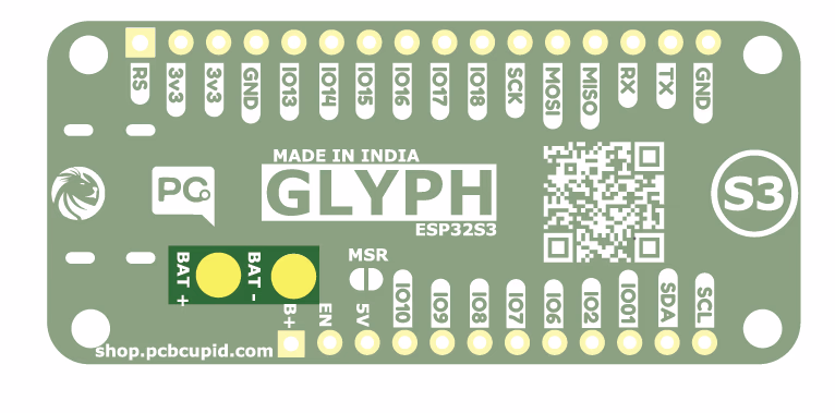
- GND: This is the common ground for all power and logic.
- BAT: This is the positive voltage to/from the Battery(+) Positive terminal (This pin is usual at voltage between 2.7v-4.2v)
- USB: This is the positive voltage to/from the USB C jack, if USB is connected (This is usual at voltage 5v)
- EN: This is the enable pin of esp32, you can pull down this using a external button or other controller to reset the board.
- 3.3V: These pins are the output from the 3.3V regulator, they can supply 900mA peak current.
- Lipo Battery PADS: 2 Pads behind the board to solder Lipo or li-ion batteries to power the Glyph board.
- MSR PADS: Short this MSR pad to measure battery capacity using IO0 (Marked as A0 on board).
Communication Pins
I2C, SPI, and UART on S3
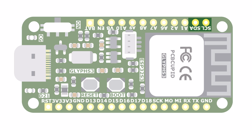
The S3 is capable of handling I2C, SPI, and UART on many pins. However, to simplify things we have assigned few of the IO pins to make things simpler for users.I2C Pins
- I2C0 SCL: SCL, IO5
- I2C0 SDA: SDA, IO4
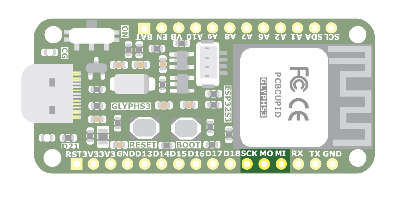
SPI Pins
- SPI0 SCK : SCK, IO35
- SPI0 MOSI: MO , IO36
- SPI0 MISO: MI , IO37
- SPI0 CS : ANY IO That’s available
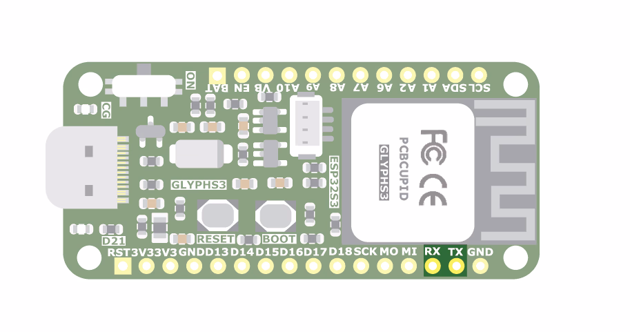
UART Pins
- UART0 TX: TX, IO43
- UART0 RX: RX, IO44
- UART1 TX: IO17
- UART1 RX: IO18
Additional Ports / Pins
Glyph Glink Port
This is a QWIIC / STEMMA compatible connector which makes it easy for users to connect to 100’s of sensors and modules made by Adafruit & Sparkfun.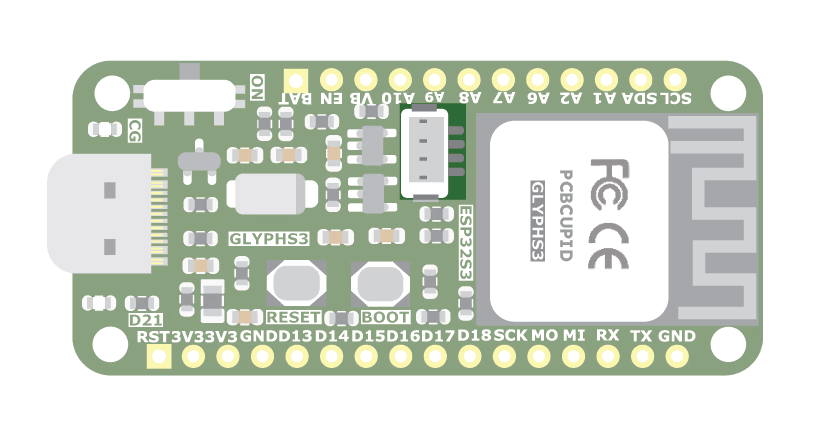
USB Pins
This is used for power and data transfer. Connect to your computer via a USB C cable to update firmware and at the USB pin you would receive 5v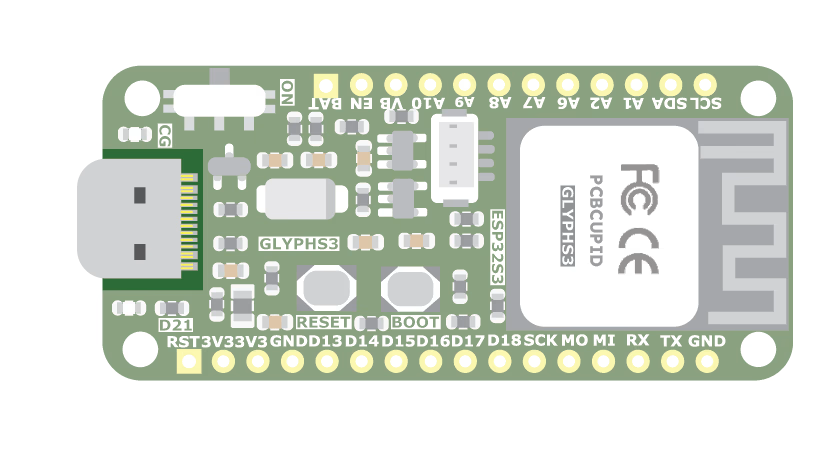
PWM Pins
The S3 supports PWM on all pins. However, it is not capable of PWM on all pins at the same time. There are multiple PWM channels, each with configurable frequency and duty cycle. The important thing to know is that you cannot use the same channel on different pins at the same time. Please refer to ESP32S3 DATASHEETAnalog Pins
The S3 has two ADC units — ADC1 and ADC2 — with 10 channels each, totalling 20 ADC-capable pins on the chip. On the Glyph-S3 board, 9 ADC1 pins are exposed: IO1, IO2, IO4, IO5, IO6, IO7, IO8, IO9, IO10- A1/IO1: ADC1 channel 1
- A2/IO2: ADC1 channel 2
- IO4: ADC1 channel 3 (Can also function as ADC1_CH3 when not used for I2C)
- IO5: ADC1 channel 4 (Can also function as ADC1_CH4 when not used for I2C)
- A6/IO6: ADC1 channel 6
- A7/IO7: ADC1 channel 7
- A8/IO8: ADC1 channel 8
- A9/IO9: ADC1 channel 9
- A10/IO10: ADC1 channel 10
Digital Pins
These are the digital I/O pins. They all have multiple capabilities but can be used only one at a time.- A1/GPIO1: ADC1 channel 1
- A2/GPIO2: ADC1 channel 2
- A6/GPIO6: ADC1 channel 6
- A7/GPIO7: ADC1 channel 7
- A8/GPIO8: ADC1 channel 8
- A9/GPIO9: ADC1 channel 9
- A10/GPIO10: ADC1 channel 10
- SDA/GPIO4: The main I2C1 data pin(GPIO4).
- SCL/GPIO5: The main I2C1 clock pin(GPIO5).
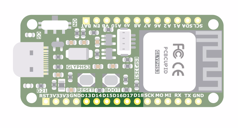
- D13/GPIO13: Digital I/O pin 13(GPIO13, FSPIIO7, SUBSPIQ, FSPIQ).
- D14/GPIO14: Digital I/O pin 14(GPIO14, FSPIDQS, SUBSPIWP, FSPIWP).
- D15/GPIO15: Digital I/O pin 15(GPIO15, U0RTS).
- D16/GPIO16: Digital I/O pin 16(GPIO16, U0CTS).
- D17/GPIO17: Digital I/O pin 17( GPIO17, U1TXD).
- D18/GPIO18: Digital I/O pin 18(GPIO18, U1RXD, CLK_OUT3).
- TX/GPIO43: The main UART0 TX pin(U0TXD, GPIO43, CLK_OUT1 ).
- RX/GPIO44: The main UART0 RX pin(U0RXD, GPIO44, CLK_OUT2).
- SCK/GPIO35: The main SPI0 SCK(GPIO35, SUBSPID, FSPID, SPIIO6).
- MO/GPIO36: The main SPI0 MOSI(GPIO36, FSPICLK, SUBSPICLK, SPIIO7).
- MI/GPIO37: The main SPI0 MISO(GPIO37, FSPIQ, SUBSPIQ, SPIDQS).
Schematic Diagram For Glyph S3
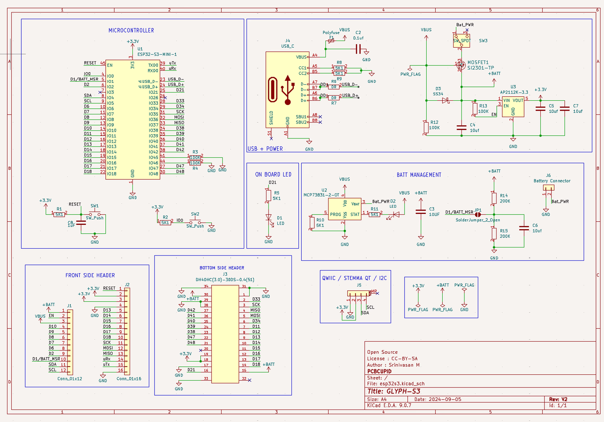
For better view you can download the schematic diagram from here